Skip to content
In the fast-paced world of technology, the need for smaller and more efficient devices is greater than ever. This drive for miniaturization, especially in the telecommunications and consumer electronics sectors, has spurred remarkable progress in antenna design. Antenna-in-Package (AiP) technology has become a vital innovation, meeting the demand for compact, high-performance antennas in contemporary devices.
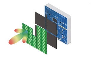
Antenna-in-Package (AiP) technology is an advanced game-changing approach that integrates antennas directly into the package of electronic devices. By embedding the antenna alongside the radio frequency (RF) chip and other essential components, AiP technology reduces the reliance on external antennas, optimizing space and improving device performance. This innovation is particularly beneficial for applications such as 5G, wearables, and automotive systems.
This innovative approach is transforming the way we design and implement antennas in modern devices, offering significant benefits across various industries. Let’s explore how AiP technology works, its benefits, and why it is becoming a crucial component in today’s high-frequency applications.
What is AiP Technology Used For?
Antenna-in-Package (AiP) technology is indeed pivotal in modern telecommunications and various high-frequency applications. Its primary uses include:

1. 5G and 6G Telecommunications: AiP technology facilitates the integration of millimeter-wave antennas, which are crucial for achieving the high data rates and low latency demanded by next-generation mobile networks. This integration enables smaller, more efficient devices that can support advanced communication protocols.
2. Automotive Radar Systems: In the automotive sector, AiP is utilized for radar systems that support advanced driver-assistance systems (ADAS) and autonomous driving features. The compact nature of AiP allows for the placement of multiple antennas in limited spaces, enhancing vehicle safety and functionality.
3. Satellite Communications: AiP technology is employed in satellite communication systems to achieve reliable and high-performance signal transmission. The compact design of AiP solutions helps optimize the space and weight constraints typical in satellite applications.
4. Internet of Things (IoT) Devices: Many IoT devices require efficient communication capabilities within a limited physical footprint. AiP technology enables the integration of antennas into small form factors, allowing for seamless connectivity in smart home devices, wearables, and industrial IoT applications.
5. Consumer Electronics: AiP is also used in smartphones, tablets, and other consumer electronics where space is at a premium. By integrating antennas directly into the package, manufacturers can save space while improving performance.

Overall, AiP technology plays a crucial role in enabling advanced communication systems and devices that require high performance in compact designs, making it a key component in the evolution of modern electronics.
How Does AiP Work?
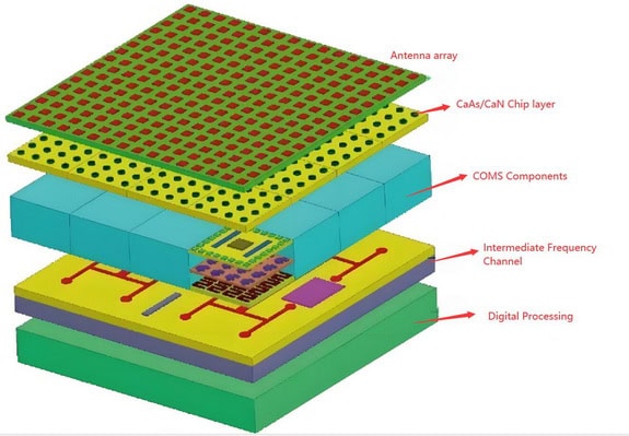
AiP technology works by integrating the antenna into the same package as the RF chip, typically on a single substrate. This substrate may include multiple layers, allowing for the creation of complex antenna structures that can support multiple frequency bands. The close proximity of the antenna to the RF chip minimizes signal losses and improves overall performance. Additionally, the use of advanced materials and manufacturing techniques ensures that the antennas can operate efficiently at high frequencies, making them ideal for cutting-edge applications like 5G.
Antenna-in-Package (AiP) technology is an innovative approach that combines antennas and RF (radio frequency) chips within a single package, streamlining the design and enhancing performance. Here’s a more detailed breakdown of how AiP works:
1. Integration: The core concept of AiP is the integration of antennas directly with RF components on the same substrate. This reduces the need for external antenna connections, which can introduce losses and degrade signal quality.
2. Multi-layer Substrates: AiP designs often utilize multi-layer substrates that allow for complex antenna geometries and configurations. This multi-layer approach can accommodate various components, including passive elements, filters, and matching networks, all within a compact footprint.
3. Minimized Signal Loss: By placing the antenna in close proximity to the RF chip, AiP minimizes the distance signals must travel, thereby reducing signal loss due to impedance mismatches and other factors. This close coupling enhances the overall efficiency of the communication system.
4. High-Frequency Performance: The use of advanced materials and manufacturing techniques, such as low-loss dielectrics and precise fabrication methods, enables AiP antennas to operate effectively at high frequencies. This is particularly crucial for modern applications like 5G, which rely on higher frequency bands for faster data transmission.
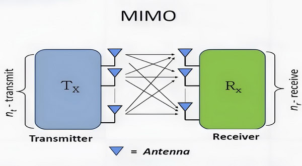
5. Multi-band Capability: AiP technology supports the design of antennas that can operate across multiple frequency bands, making it suitable for devices that require versatility, such as smartphones and IoT devices. This capability is achieved through innovative antenna designs, such as MIMO (Multiple Input Multiple Output) configurations.
6. Compact Design: The integration of antennas within the package allows for a more compact overall design, which is essential for modern electronic devices that demand miniaturization without compromising performance.
7. Cost Efficiency: By reducing the number of discrete components and simplifying the assembly process, AiP can lead to lower manufacturing costs and increased reliability, as there are fewer connections that can fail.
In summary, AiP technology represents a significant advancement in RF design, enabling high-performance antennas to be integrated directly with RF chips in a compact and efficient manner, making it particularly well-suited for next-generation wireless communication systems.
What Are the Benefits of AiP?
Antenna-in-Package (AiP) technology offers several benefits, particularly in the fields of telecommunications, IoT devices, and consumer electronics. Here are some key advantages:
1. Space Efficiency: AiP integrates the antenna directly into the package of the semiconductor, significantly reducing the overall footprint. This is particularly beneficial for compact devices where space is at a premium.

2. Improved Performance: By minimizing the distance between the antenna and the chip, AiP can enhance signal integrity and reduce losses. This leads to better communication performance, including higher data rates and improved range.
3. Design Flexibility: AiP allows for more flexible design options, enabling manufacturers to create innovative and compact device designs. This is especially important for wearable technology and other miniaturized devices.
4. Reduced Manufacturing Complexity: Integrating the antenna within the package can simplify the assembly process, reducing the number of components and potentially lowering manufacturing costs.
5. Enhanced Reliability: With fewer external connections and components, the risk of mechanical failure or signal degradation due to environmental factors is reduced, leading to more reliable devices.
6. Multi-Band and Multi-Mode Capability: AiP can support multiple frequency bands and communication protocols in a single package, enabling devices to operate across various networks (e.g., LTE, 5G, Wi-Fi) without needing multiple antennas.
7. Lower Cost of Ownership: While initial costs may be higher, the overall cost of ownership can be lower due to reduced assembly complexity, improved performance, and lower failure rates, which can lead to lower warranty claims and maintenance costs.
8. Better Aesthetics: AiP can contribute to sleeker, more aesthetically pleasing device designs, as it allows for the integration of antennas without the need for protruding elements.
9. Scalability: AiP technology can be easily scaled for different applications, from consumer electronics to industrial IoT devices, making it a versatile solution for various markets.
10. Support for Advanced Features: AiP can facilitate the integration of advanced features such as beamforming and MIMO (Multiple Input Multiple Output), which are essential for enhancing wireless communication capabilities.
Overall, AiP technology represents a significant advancement in antenna design and integration, providing numerous benefits that align with the evolving demands of modern electronic devices.
What Does the AiP Consist Of ?
AiP (Antenna-in-Package) technology comprises several essential components:
1. Antenna Elements: These are the antennas themselves, specifically designed to function at designated frequencies and integrated directly into the package substrate.

2. RF Chip: This is the primary component responsible for generating and processing radio signals. It is strategically positioned near the antenna elements to reduce signal loss.

3. Substrate: Serving as the foundational material, the substrate accommodates both the antenna elements and the RF chip. It often features multiple layers to facilitate intricate antenna designs.
4. Interconnects: These electrical connections link the antenna elements to the RF chip and other components within the package, ensuring proper signal transmission.
In addition to these core components, AiP technology may also include:
5. Passive Components: This category encompasses resistors, capacitors, and inductors integrated into the package to aid in signal conditioning and filtering, thereby enhancing overall performance.
6. Thermal Management Solutions: Depending on the application, thermal management features may be incorporated to maintain the RF chip and other components within safe operating temperatures.
7. Shielding: To reduce interference from surrounding electronic components and improve performance, shielding materials may be integrated into the design.
8. Packaging Materials: The selection of materials used for packaging can significantly influence performance characteristics, such as dielectric constant and loss, which impact the antenna’s efficiency.
9. Testing and Calibration Features: Some AiP designs may incorporate built-in features for testing and calibration, ensuring optimal performance in final applications.
10. Integration with Other Technologies: AiP can also be combined with other technologies, such as MEMS (Micro-Electro-Mechanical Systems) or advanced semiconductor technologies, to create more compact and efficient designs.
Overall, AiP technology aims to deliver a compact, efficient, and high-performance solution for wireless communication systems, particularly in applications like smartphones, IoT devices, and other wireless-enabled products.
Why is it Necessary to Use AiP ?
The necessity of AiP technology arises from the growing demand for high-frequency operation and the shrinking size of modern electronic devices. Traditional antenna designs are often too large or inefficient for use in compact devices like smartphones or wearables. AiP technology addresses this issue by providing a space-efficient solution that does not compromise on performance. Additionally, as communication standards continue to evolve towards higher frequencies, the ability to integrate complex antenna structures within a single package becomes increasingly important.
Future Implications of AiP Technology
Antenna-in-Package (AiP) technology has significant implications for the future of wireless communication, particularly in the realms of WiFi, 5G, and the upcoming 6G standards. Here are some potential future implications:
1. Increased Integration and Miniaturization
– Space Efficiency: AiP technology allows for the integration of antennas within the semiconductor package itself, leading to smaller form factors for devices. This is particularly beneficial for IoT devices, wearables, and smartphones, where space is at a premium.
– Advanced Packaging Techniques: The use of advanced packaging techniques, such as System-in-Package (SiP) and 3D packaging, can further enhance the integration of multiple functions, including processing, memory, and RF components.
2. Enhanced Performance
– Improved Signal Quality: AiP can reduce the distance between the antenna and the RF front end, minimizing losses and improving overall performance. This is crucial for high-frequency applications like 5G and 6G, where signal integrity is paramount.

– Higher Frequency Support: As wireless standards evolve to higher frequencies (e.g., mmWave for 5G and beyond), AiP technology can facilitate the design of antennas that operate effectively in these bands, supporting higher data rates and lower latency.
3. Support for Advanced Applications
– Massive MIMO and Beamforming: AiP can support advanced antenna technologies like Massive MIMO (Multiple Input Multiple Output) and beamforming, which are essential for enhancing capacity and coverage in dense urban environments.
– Smart Antenna Systems: The integration of AiP with smart antenna systems can enable adaptive beam steering and improved spatial diversity, enhancing user experience in applications such as augmented reality (AR) and virtual reality (VR).

4. Cost-Effective Solutions
– Reduced Manufacturing Complexity: By integrating antennas into the package, manufacturers can reduce the number of components and assembly processes, leading to cost savings and potentially lower prices for consumers.

– Economies of Scale: As AiP technology matures and adoption increases, economies of scale may drive down costs, making advanced wireless technologies more accessible to a wider range of applications and markets.
5. Sustainability and Energy Efficiency
– Lower Power Consumption: AiP technology can contribute to lower power consumption in devices by optimizing the RF front end and reducing signal loss, which is essential for battery-powered devices.

– Eco-Friendly Materials: The development of new materials and processes for AiP can lead to more sustainable manufacturing practices, aligning with global efforts to reduce electronic waste and environmental impact.
6. Enhanced Connectivity for IoT
– Scalability for IoT Devices: With the proliferation of IoT devices, AiP technology can provide the necessary scalability and performance to support a massive number of connected devices, enabling smart cities, industrial automation, and smart homes.

– Seamless Integration: AiP can facilitate seamless integration of communication technologies, allowing IoT devices to operate across multiple standards (e.g., WiFi, 5G) without the need for multiple antennas.
7. Future-Proofing Wireless Technologies
– Adaptability to New Standards: As wireless communication standards evolve, AiP technology can be adapted to meet new requirements, ensuring that devices remain relevant and capable of supporting future applications.
– Research and Development: Ongoing R&D in AiP technology will likely lead to innovations that further enhance performance, reliability, and functionality, paving the way for next-generation wireless applications.
In summary, AiP technology is poised to significantly impact the future of wireless communication by enabling higher performance, greater integration, and enhanced capabilities for WiFi, 5G, and 6G networks. As the demand for connectivity continues to grow, the role of AiP will become increasingly critical in shaping the landscape of modern communication technologies.
Summary
The development of Antenna-in-Package (AiP) technology has revolutionized antenna design by providing a compact and high-performing solution for modern electronic devices. AiP technology overcomes the limitations of size reduction and high-frequency operation by integrating the antenna within the same package as the RF chip. As this technology advances, it will become a critical component in the creation of future communication networks and advanced electronic systems.